
In an era where artificial intelligence is accelerating faster than ever before, the world’s dependence on computing power has reached unprecedented levels. Data centers consume enormous amounts of electricity, semiconductor manufacturers are approaching the physical limits of silicon, and the race for faster, more sustainable technology has become one of the defining challenges of modern civilization.
Against this backdrop, on April 23, 2026, Dr. Ko-Cheng Fang, Founder and CEO of LongServing Technology, officially unveiled a groundbreaking series of photonic chip architectural designs through the company’s official platform. The release included a 3D architectural schematic of the photonic chip, a complete photonic pathway system architecture, and, for the first time publicly, a structural demonstration of a photonic full-adder chip.

The unveiling marks a major milestone in the evolution of next-generation computing. Unlike conventional electronic chips that rely on electrons traveling through metallic circuits, photonic chips use light itself—photons—to transmit and process data at extraordinary speed with dramatically lower energy consumption.
According to Dr. Fang, the newly revealed architecture introduces a complete redesign of computational structure, one that could potentially move humanity beyond the limitations of traditional semiconductor technology.
At the heart of this breakthrough is a radically different approach to chip engineering.
Traditional electronic chips require dozens of stacked fabrication layers, increasingly complex lithography systems, and immense power consumption to sustain modern AI processing demands. Dr. Fang’s photonic chip architecture instead adopts a three-layer integrated structure specifically optimized for light-based computing.

The bottom layer functions as photonic memory, enabling the direct storage of optical signals. The middle layer houses photonic logic gates responsible for computational operations. The top layer is dedicated entirely to photonic pathways, through which photons travel across the chip architecture.
Most notably, the entire photonic circuit system has been redesigned into a 45-degree optical pathway configuration, a departure from traditional planar chip layouts. This configuration demonstrates the stacking capability of the photonic chip while maximizing the efficiency of optical signal transmission.
Each layer is fabricated using three independent photomasks, significantly simplifying structural complexity compared to conventional semiconductor manufacturing.
For photonic systems, this three-layer architecture may already be sufficient to achieve extraordinary computational capability, eliminating the need for the massive multi-layered structures used in electronic chips today.

Dr. Fang describes this as more than simply a new chip design. He sees it as the beginning of a technological transition that could reshape the future of artificial intelligence, robotics, cloud computing, and sustainable global infrastructure.
One of the most remarkable aspects of the announcement is the integration of photonic memory into the computing architecture itself.
Current semiconductor systems constantly convert electrical signals into optical signals and back again during data transmission. These repeated conversions create inefficiencies, heat generation, and energy loss. By integrating photonic memory directly into the chip system, LongServing Technology aims to dramatically reduce these conversion bottlenecks.
The result, according to the company, is computational performance potentially reaching hundreds of thousands of times faster than conventional electronic chips.
Yet Dr. Fang argues that the true upper limit may be impossible to measure accurately because of the instantaneous nature of light-speed data access itself.
This concept builds upon Dr. Fang’s earlier development of a 2-nanometer photonic quantum material known as “X-Photon,” a breakthrough material specifically engineered for nanoscale photonic pathways and next-generation photonic quantum chips.

The X-Photon material has become one of the core foundations of LongServing Technology’s photonic computing ambitions. Unlike traditional silicon photonics operating at relatively large wavelengths, the X-Photon system seeks to dramatically reduce wavelength size to enable ultra-dense optical circuitry compatible with nanoscale chip fabrication.
For years, one of the biggest barriers to practical photonic computing has been wavelength limitation. Conventional silicon photonics typically operate at wavelengths between 1300 and 1500 nanometers, far larger than the dimensions required for modern semiconductor circuits.
Dr. Fang’s work attempts to address this challenge by engineering ultra-short wavelength photonic materials capable of functioning at approximately 2 nanometers, pushing optical computing closer to the scale required for next-generation AI systems.
In many ways, this announcement represents the culmination of years of independent research and unconventional thinking.
Dr. Fang’s journey into advanced technology has never followed a traditional path. Widely recognized as an inventor, scientist, entrepreneur, and artist, he has worked across multiple fields ranging from cybersecurity and cloud computing to laboratory-grown Imperial Green jadeite and biotechnology research.

Earlier in his career, he developed cloud storage and programmable password lock technologies later adopted by the U.S. Department of Homeland Security, contributing to modern information security and cloud infrastructure systems.
But it is photonic quantum computing that he believes may ultimately define humanity’s next technological era.
Dr. Fang frequently speaks about the growing environmental burden of modern AI infrastructure. Massive data centers now consume enormous quantities of electricity, while semiconductor fabrication itself demands increasing energy resources and cooling systems.
According to him, continuing to scale traditional electronic chips indefinitely is no longer sustainable.
Photonic computing, by contrast, offers the possibility of dramatically reduced heat generation, lower carbon emissions, reduced electromagnetic interference, and computational speeds far beyond the capabilities of today’s semiconductor processors.
The implications extend far beyond faster computers.
If scalable, photonic quantum chips could transform industries including autonomous vehicles, AI robotics, telecommunications, advanced scientific simulation, medical systems, aerospace engineering, and global cloud infrastructure.
Dr. Fang envisions a future in which photonic quantum systems power truly intelligent robotics, interconnected AI networks, and next-generation automation systems operating at speeds impossible for conventional semiconductor technology to achieve.
At the same time, LongServing Technology is actively seeking global semiconductor manufacturing partners to accelerate implementation and commercialization of photonic quantum chip production.

Rather than competing directly against existing semiconductor foundries, Dr. Fang advocates for collaboration—allowing current fabrication facilities to transition gradually into hybrid electronic-photonic manufacturing platforms.
This approach could potentially enable the industry to evolve without completely rebuilding global semiconductor infrastructure from the ground up.
For Taiwan, the implications are particularly significant.
As one of the world’s most important semiconductor manufacturing hubs, Taiwan stands at the center of the global AI and chip economy. Yet the island also faces growing concerns surrounding electricity demand, energy sustainability, and the long-term physical limitations of silicon-based technology.
LongServing Technology’s announcement positions Taiwan not only as a leader in semiconductor manufacturing, but potentially as an early pioneer in the transition toward photonic quantum computing.
Beyond the technical achievement itself, the unveiling also reflects Dr. Fang’s broader philosophy regarding innovation.
He often describes invention not as a pursuit of short-term profit, but as a responsibility to humanity’s future. Whether through biotechnology research, environmental sustainability, or photonic computing, his work consistently emphasizes long-term societal transformation over immediate commercial gain.
For him, photonic quantum chips are not simply faster processors.
They represent a possible answer to one of humanity’s greatest technological challenges: how to continue advancing artificial intelligence and computational capability without exhausting the planet’s energy resources.

As AI systems continue expanding into every corner of human life, from medicine and transportation to finance and robotics, the demand for faster, cleaner, and more efficient computing will only intensify.

The unveiling of LongServing Technology’s photonic chip architecture may therefore represent more than a scientific announcement.
It may be an early glimpse into the next chapter of civilization’s technological evolution—one where light itself becomes the foundation of computation.
And if Dr. Ko-Cheng Fang’s vision proves successful, the future of computing may no longer belong to silicon alone, but to photons traveling at the speed of light.
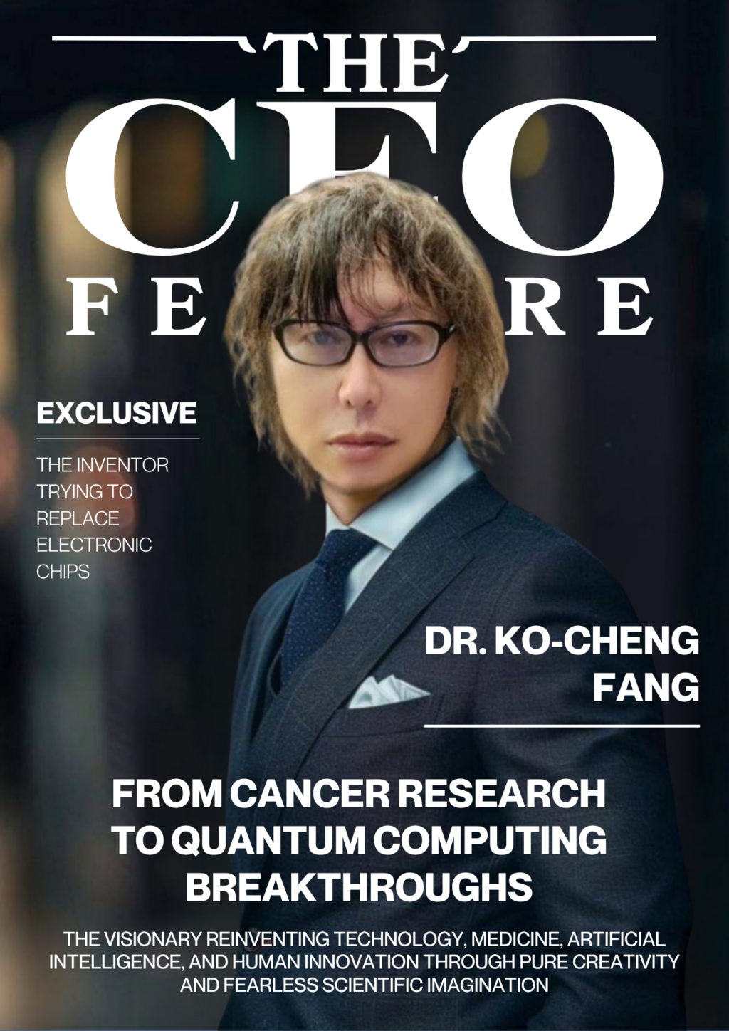
Dr. Ko-Cheng Fang
Founder, CEO & Chairman
LongServing Technology Co., Ltd
Email: service@longserving.com.tw
Website: https://longserving.com.tw/en/
Instagram: @ko_cheng_fang_david